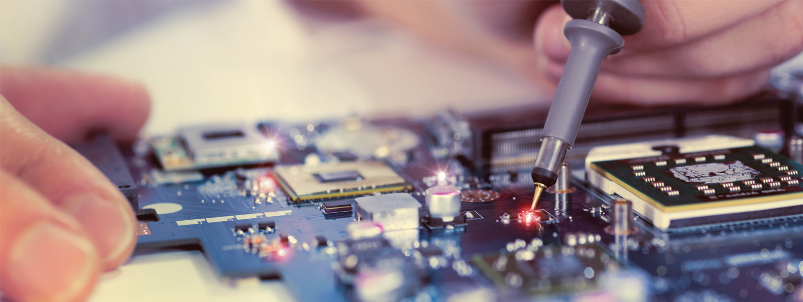
May 17

SMT Soldering–It’s easier than you think! is our new Manga Comic that shows you step by step tips and techniques for learning to solder SMT parts.  To down load the full comic press on the comic front page:

                            SMT_Soldering_Its_Easier_Than_You_Think010001

We’d love to get your feedback on the comic.  We are in the process of working out the kinks so we can get translations of the comic into everyone's hands – we’ll keep you posted.

For everyone that learns better with hands on experience we are offering our SMT 2D6 SMT Learn to Solder Kit in the store. You will end up with a 2 Dice simulator that can be used for games and fun and satisfaction in your new found knowledge that you gained in the world of SMT electronics.


                                     DSCN1160


Have fun – let us know what you think

SoftwareSodbuster

Tags:
Apr 02

If you had any doubts that SiliconFarmer has an actual farm, this project should dispel them. We got six chickens last year.  I built them a nice coop. It sits about 100 feet from the house, and has wheels so we can occasionally move it.

Chicken coup for six

Chickens like to be in the coop at night.  They are protected from predators, and they can stay warm if there are no drafts. They like to be outside during the day to forage for food.

This means someone has to go out early in the morning to open the coop, or they get noisy and start pecking each other.  And after it gets dark, someone has to go out to close the door so they are protected, regardless of the weather. Did I mention it is after dark?

Anyway, this gets old after a while.  So I built an automated system to open the door at dawn, and close it at dusk.

Design

The first problem was deciding what sort of motor and mechanism to use.  Brent from Autosport Labs suggested using a window wiper motor, as they are 12V, high torque, geared about the right speed, and can be found cheap at a junk yard.

Subaru window wiper motor

He also suggested using an arm and pulley mechanism so the motor could be run in just one direction to both open and close the door.

These motors have an integrated switch, which allows my controller to determine when the motor is positioned with the door completely closed. 

The completely open position isn’t as critical. No one cares if the door is an inch down from the absolute top.  So I can use a simple timing loop for opening the door.

Motor reverse engineeringFirst thing I did was figure out which leads ran the motor, and which was the feedback switch.  Ohm meter, 12V battery, and an oscilloscope made quick work of that.

One lead is common, two leads are power for slow and fast speeds.  I used the slowest speed – fast was too fast! The forth lead comes from a switch connected to common that is only closed at one position. 

The motor is rated at 10 amps, and I had a 10A 12V relay in my parts drawer, so I chose to use a relay instead of a transistor to control the motor. 

It still took a small NPN transistor and flyback diode to control the relay.  I checked out all the circuits, one by one, on a breadboard before I created my schematic and had the boards built by @laen’s PCB prototype service.

I decided to use an Arduino with a custom shield design for this project.  As I tried out circuits, I wrote quick little bits of Arduino code to test them. To create the final software code, I had working snippets of code from my testing to use for each function.

My Chick Door Shield has the following features:

  • SPST 10A 12V relay to drive the motor.
  • NPN transistor and flyback diode to drive the relay.
  • An opto-isolated input to sense the motor’s switch.
  • 12V battery input. This goes through a polarity protection diode to the Arduino’s VIN.  the Arduino’s regulator generates 5V. The Arduino uses an inefficient regulator, so in hind sight, I wish I’d put a 5V regulator with lower quiescent current on the shield. 
  • Voltage divider input on the 12V battery to check battery charge level.  3:1 ratio so the input is good to 15V.
  • Voltage divider input on the solar panel.  Again, 3:1 ratio input.  This might be too low, as some unloaded solar panels can hit 18 volts.
  • A PFET to connect the solar panel to the battery. This is to avoid over-charging the battery.  Also, solar panels can drain a battery when there isn’t sufficient sun.  Even a solar panel with a protection diode will have a leakage current. With a PFET oriented the correct way, there is no leakage at all.
  • An input from a button, so the door can be manually operated.
  • I threw on a temperature sensor and a spare connector and power to an IO pin.  I plan to  eventually add a radio so I can monitor the door position, and check it with a limit switch or optical sensor.  I could also monitor the coop temperature.

ChickenDoorSchematic

I built the board, mounted the motor to a bit of metal and attached the arm.  Then I tested it on my workbench.  Everything worked!  I also debugged my software on the workbench.  One thing I found out was that the motor really does have a lot of torque.  You don’t want it to hit anything! 

P1000657

Software features

  • The motor switch input pin fires an interrupt, which immediately shuts off the motor. This gives me the best accuracy on repeatedly positioning the arm in the same spot when closing the door.
  • The closing the door function uses a delay(500*3) followed by another motor shut off, just in case something happens to the wire from the switch.  I don’t want to run the motor until the battery dies!
  • The current surge from starting the motor can cause noise spikes from the motor power leads coupling to the switch wire.  This could inadvertently stop the motor too soon. So the close door function also delays arming the motor switch interrupt for 10mS after starting on the motor.
  • The open direction is controlled by a simple delay(500). This opens the door a bit past fully open.  I figure if the door sticks a little, it won’t open quite as far as expected, which should still be OK.
  • The light level (reading from the solar panel) is set to 50 for sensing night.  That’s under a 1V output from the 12V solar panel.  The chickens don’t go into the coop until after sundown, so I figured that on a cloudy day, I need to wait until as late as possible to close the door.
  • The open light level is set to 100, plus a 5 second debounce period.  This is to add some hysteresis so the door doesn’t go up and down repeatedly, and to avoid lightning flashes from opening the door.  It probably wouldn’t hurt to raise it to 200.
  • The FET is off when I check the battery and solar panel voltages.  It is on only when the solar panel voltage is higher than the battery voltage, and the battery isn’t over 14.6 volts.
  • All interesting values are checked for changes, and output on Serial.Print every control loop (10ms).  All I have to do is hook up to the USB port to see what is going on.  Eventually, I can connect a radio to the Arduino UART pins and get status messages from the chicken coop.

Hardware build

The control electronics are in a case, right next to the battery, in a storage area under the chicken roost.  It is dirty down there.

P1000847

The solar panel on the roof is a spare 10W panel. If there is any sun at all, the battery gets charged.P1000839

The manual push button is mounted right by the door.  You can see the plastic sleeve going through the wall of the coop so the paracord doesn’t get frayed, and the pulley that pulls the door up and down.

P1000838

Here is the pulley on the inside, with the paracord heading out through the plastic sleeve. As the arm swings around in its arc, this pulley makes sure the cord is going straight out through the hole in the wall

P1000842

Here is the motor, mounted to the ceiling, in the open position.  When closed, the arm is pointing at the camera position, toward the inside pulley.

P1000844

An overall picture of the arrangement of the motor and indoor pulley. You can see the cable going to the motor run along the rafter.  Don’t put cable (or anything else) where a chicken can peck at it. Eventually, they will damage it if they can get to it.

P1000841

I have some video of the automatic chicken door in action, but I need to edit it down and upload it to Youtube, then I will update this page.

Tags:
Mar 03

Disclaimer: I am not a lawyer. These are my notes from some presentations I attended and some help from Google. This material only covers U.S. copyright.

You don’t have to put a notice on your work, nor do you have to register it with the U.S. Copyright Office to have copyright protection.  But doing those things does give you some benefits. 

Copyright notice

A copyright notice provides three benefits:

  • helps scare away potential infringers
  • it prevents the claim of “innocent infringer” which limits penalties
  • identifies you so that someone can contact you to request a license

To be a valid notice, the copyright notice must have the following:

(1) the symbol © (the letter C in a circle), or the word “Copyright”, or the abbreviation “Copr.”

(2) the year of publication.

(3) the name of the owner of copyright, or an abbreviation by which the name can be recognized, or a generally known alternative designation of the owner.  For example “siliconfarmers.com” would be considered a “generally known alternative”.

(4) the copyright notice has to be placed so it can be seen. This include machine readable forms, such as video or text.

Note that  “(c)” cannot be used in place of © in a valid notice.  Also, “All rights reserved” is not needed.

Copyright registration

Copyright registration provides several benefits, including:

  • If you register within 3 months of publication, it is possible to collect statutory damages (up to $150,000) and attorney fees. Otherwise, you can only collect actual damages (lost revenue) and 2X the license fees that should have been paid.
  • If you register within 5 years of publication, the registration can be used as your evidence in court of the validity of the copyright.
  • Registration is needed for recording the transfer of ownership of the copyright.
  • Registration allows the copyright to be used to prevent the importation of infringing copies.
  • You have to register before filing a civil or criminal case against an infringer.

There are criminal penalties for copyright infringement. Unfortunately, it is limited to a fine of only $2500, and the statute of limitations is 5 years.

US Copyright registration requires just three things:

  • A form you can complete online. You have to first create user login, of course.
  • A copy (or two) of the work to be registered.  The copy can be in electronic form. They accept a wide variety of file formats.
  • A $35 filing fee, which is payable on-line by credit card.

To register online, you start at the home page of the US Copyright Office.

The US Copyright office also provides a large FAQ on copyright.

Tags:
Feb 28

Some people never use hotkeys and stick with menus.  I find hotkeys to be a good productivity tool.  One hand running the mouse while the other chooses the next function is a considerable time saver when you think about all the commands you have to select while using a PCB CAD tool.

Unfortunately, Eagle CAD has a small issue with hotkeys. You can’t assign them to the alphanumeric keys except when used with <ctrl> or <alt>  Personally, I find it easier to just run the mouse to the toolbar than find ctrl-whatever to invoke a command.  That leaves me with the function keys.  The function keys in Eagle CAD support un-shifted, <shift>, <alt>, and <ctrl>, but stretching my fingers from a <shift> key to function keys is also not easy, so I use the shifted function keys sparingly.

With only 10 or 12 function keys available, you need to consider what functions you use the most often, and put those on the un-shifted function keys.  When I’m routing a board, I’m constantly switching between route, move, split, and ripup.  So I put those right in the middle of the function keys.

There are also some things that are done less frequently, but are a pain to configure.  I put switching the grid from mil to mm and setting which layers to view on function keys.  I use F12, for example, as my key for selecting layers.

F12 un-shifted is all of the routing layers, shift-F12 is only the top layers, ctrl-F12 is only the bottom layers. alt-F12 selects the assembly layers so I can do a printout to help me with assembly. When I’m finalizing the silkscreen, I don’t care about routes, but I want to avoid pads, vias, and pins, so I have alt-F11 to select those layers as visible.

Here are my function keys:

Eagle function keys

There are three ways to define your function keys.

First, you can use the menu Options > Assign to bring up a window that will allow you to change hotkey assignments while in Eagle and try them out. When you quit, those settings will be saved only for the current project.

You can program your hotkeys by putting commands into your startup script file scr\eagle.scr in your Eagle program directory. This is how you change your hotkeys and have them apply to all your projects.  It is best to try them out in a project first to make sure they work.

Finally, if you want to change some or all your function keys, or load someone else’s hotkey assignments, you can run a script to change them.

To help me remember my hotkey assignments, I use a spreadsheet to make a paper template that sits above the function keys.  I have them almost memorized, but I like to have an easy reference available right above the keys to keep me productive.

P1000744

Tags: |
Feb 18

Devices are how you tie the schematic symbols to the packages (footprints) in Eagle CAD.

I’m not going to cover the basics of creating devices, which is covered quite well in Sparkfun’s tutorials and elsewhere.  Here are some slightly more advanced tips on creating devices.

Devices

1.       If you add more than one package to a device (using the New button on an existing device), you will have to define the “Variant” text. Manufacturers often put letters and numbers at the end of a part name to designate it’s package type, for example DIP package might be “-PU” and SMT “-SU”. You might want to use what the manufacturer uses, as it can help with parts ordering. Or you can just use your package name (“-DIP8”, “-SOIC8”).  If you want to change the name of a variant, just right click it and select “Rename”.

image


2.       Set “Value” On (look for a radio button) if you want to be able to set the value of each instance of this device in the schematic, such as “100” for a resistor.  If you leave it Off, you are stuck with the Device name (“ATTINY45”) concatenated with the Variant text, if any.  If the variant is set to “-SOIC8”, then “ATTINY45-SOIC8” will be the “Value” on the schematic and layout (and parts list).

image


3.   Don’t forget to click the Prefix button and put in the character you want to see for the devices first letter as the start of its reference designator.  For example R for resistor and U for IC.  Multiple characters are allowed, such as JP for jumper.

4.       The “Description” field shows up when you are looking through a library file, trying to find the right part to put on your schematic.  You can put anything you want here by clicking on Description.  Make sure it is something that will help you identify the right part as you look through your device list.  For example, the Device might be “2N2907” and the Description would be “Generic small signal PNP transistor”.

image


That wraps up my series on Eagle CAD libraries.  I hope you got some tips that will help you improve you skill with Eagle CAD libraries.


Tags: |
Feb 05

Now that I’ve covered symbols in Part 2, I’m going to talk about Eagle CAD packages. 

What Eagle CAD calls “packages” are also called footprints and land patterns.  I commonly say the word “footprint”, so please bear with me for switching around occasionally.

What follows is a list of tips that will help you be more efficient and less error prone in the long run, at the expensive of a little time upfront while designing your footprints.  I mean packages.

Package Tips

1.       Put the origin of the footprint near physical centroid of the body, and positioned to keep pads on-grid if possible.  This makes placing and rotating parts easier during layout.  If one of your board designs becomes wildly popular and you need it mass produced, it will be easier to automate production if you have followed this rule.

2.   Some devices will have a “Recommended PCB mounting pattern” near the end of the datasheet. Follow that when available.  Use your calculator to figure out the absolute locations of the pads and use the Info command to pull up the Properties dialog and enter in the coordinates of the pads by hand. 

padProperties

      Don’t be afraid to stretch surface mount pads out a 0.5 to 1 mm to make it easier to hand solder.  If the datasheet doesn’t have a suggested footprint and you are at a loss for finding an example, you could try the IPC Land Pattern Calculator.  See below for more info on this tool.

3.   PAD Thermals and Stop boxes should be check marked as active.  For SMT pads, Cream should also be check marked.

4.       Put pin one on the left for 2 pin devices (positive for polarized caps or cathode for diodes), and in the upper left for most ICs. Top center is used for ICs that have pin 1 in the center of a side (PLCC). This also helps with automated production.

5.       Mark pin 1, either in copper using a different pad shape, such as square, and/or the silk screen with a dot or a “1”, or place a distinctive nick in the outline to match the package. Most libraries mark the positive pin on polarized caps with a “+”, and use a line to mark a diode’s cathode.  I like to do that plus change the pad shape.  Sometimes, the silkscreen won’t be visible due to crowding or parts overlaying it, so the double indication can be helpful.

ExampleFootprint1

6.   Always place “>NAME” and “>VALUE” in the Name (25) and Value (27) layers.

7.       Text should be at least .032”, I use 0.05” for text in the library, then Smash and Info to shrink the text in layout if needed for space.

8.       Make a nice part outline that reflects the body shape of the part for the silkscreen in layer tplace (21). It doesn’t have to be super accurate, it is just used for guiding hand assembly. Use layer tplace (21) for the part outline to get it to appear in the silkscreen.  Don’t be afraid to be artistic!  You and everyone else are going to see this on your board.

2contactscrewterminal

9.   Use layer tDocu (51) to add information that will help you during assembly.  For example, instead of the little line to indicate polarity of a diode, put in a triangle-and-line diode symbol so there is no doubt about polarity when looking at a printout of the tDocu layer.  Use tDocu to give a complete outline of your parts, so it is clear during assembly where everything goes.

10.  Layer 39, tKeepout, is used by the DRC function to check that parts are not too close.  For most through hole parts, it isn’t necessary to use this as the silkscreen and pads will keep things spread out.  But you should create a tKeepout on SMT parts to make sure you have left enough room for tweezers between parts and a soldering iron tip between pads.  During layout, you can loose track of the scale of things and get things too close together. tKeepout plus using the DRC function will keep you out of trouble.  0.5mm on the sides of a part will give you 1mm for the end of a tweezer between parts.  You might want 1mm out from pads to keep parts 2mm apart to leave room for your soldering iron.  

11.       Avoid naming a footprint for a specific part. Using a name that describes the footprint shape rather than the function of the device will help you find it when you need it for another part, saving you the time and effort of recreating the same footprint.  

LibraryDescriptions

12.  Click on Description to give more information about the package. For example, “Electrolytic Capacitor type A SMD”. If you work in the lower half of the Description popup, you can use markup language on the text.  For example <b></b> for bold, and <p> for paragraph breaks.

13.      Follow a systematic naming scheme for footprints. This should be designed to help you quickly find and reuse footprints in your library. Try to make the name so descriptive you won’t have to look at the package graphics to tell if it is the right footprint. Don’t be afraid to use a long name. 


For IC’s, you can often just use the package type.  For example SOT23, SOIC14, QFN32.

For resistors, capacitors, LEDs, and other parts that come in a variety of footprints that will be associated with a single schematic symbol, I suggest using a letter or two or three for the type of part: R, C, LED, CP for polarized capacitors, and so on.  Then designate the size.

Choose a convention and stick to it. For example, Adafruit’s Eagle CAD library names large capacitor footprints with C, followed by the pin spacing in 0.1mm, a dash, then the outline X-Y size in 0.1mm.  For example: C225-074X268.  It makes finding a large capacitor shape very easy in her library.


IPC Standards

If you want to design footprints like the pros, check out the IPC Standards Organization.  IPC members are professional layout designers and manufacturing engineers that have a lot of experience in what works and what doesn’t for PCB footprints.  They put lifetimes of knowledge and expertise into the standards.  Some of the standards are available for free, others are somewhat expensive.

They have a five page document on their footprint naming convention. I see professional layout designers using it all the time.  But its more than I bother with.

You can probably find a copy of their (slightly outdated) IPC-SM-782A standard online. 288 pages of surface mount land pattern info that only a layout geek could enjoy.

IPC782A

If you end up with a part that doesn’t have a recommended footprint in its datasheet, a better option might be the IPC Land Pattern Calculator.  It is available for free with registration. It can create a datasheet with the footprint you need (if you feed it all the data it needs).  I have used it a few times.  It is not something you would want to do for every new part you use.  Their Land Pattern Wizard can actually output footprint data files, but it requires an expensive license.

PCBCalculator

Footprint Trivia

Have you ever wondered why people create separate R0603 and C0603 footprint shapes?  Those devices are the same shape, right?  Not quite.  Surface mount resistors are usually fairly low profile: they are “flat”. While capacitors usually have a square profile: they are as tall as they are wide. In high volume automated production, the optimal pad size is partially determined by the height of the component. For hand soldering you will probably want a somewhat larger pad than for automated assembly.  Using Adafruit’s library again as an example, she provides four footprints for “0805” devices: R0805 and C0805 for hand assembly, R0805W and C0805K for automated assembly.

Tags: |
Jan 26

In Part 1, I talked about re-using parts from publicly available libraries.

In this post, I’m going to give a few pointers on creating good symbols. Symbols are relatively easy to do,  so this will be short.

If you are completely unfamiliar with making symbols, I suggest reading the Sparkfun tutorial on creating new parts in Eagle CAD.

Schematic Symbol Tips

  1.  Make sure the pin connection points (green circles) and the symbol’s origin are on grid (0.1”).  Best way to do this is to not change the grid.  If you need to tweak the location of silkscreen objects, press alt while dragging or move it by typing in the coordinates using the object properties (via the i icon). If a pin connection point gets off grid, it is very hard to get wires to attach. 
    • If you end up with a pin that is off-grid, use Info to open the properties of the pin and manually change the pin Position to a location that is on the 0.1 grid.
  2. Don’t forget to put “>NAME” (layer 95, usually at the top of the symbol) and “>VALUE” (layer 96, usually at the bottom of the symbol)
  3. To create multiple pins with the same name, name them “@” and then a number.  Example: if you name pins GND@1 and GND@2, then only “GND” will show on the schematic for those pins.
  4. The origin of the symbol should be near the center.  This make rotations and mirroring more convenient.
  5. Don’t be shy about copying symbols from other libraries.  Symbols are a lot easier to get right than footprints.  It is also handy when creating a new part that is similar to one already in a library.  Often all that is needed to create a new part is to copy an old symbol and fix up the pin names.  But Eagle doesn’t make it easy to copy just a symbol.

You can’t use the Control Panel to browse symbols, so there is no drag and drop method for copying symbols.  You have to use copy/paste.

Here are the detailed steps for copying a symbol from an Eagle CAD library to your library. 

Copying an Eagle CAD symbol

  1.  
    1. Open the source library

    2. Find and open the symbol you want to copy

    3. Use Group tool to select the whole symbol

    4. Then select the “cut” tool, which looks like scissors. Don’t worry, it doesn’t remove anything from your source.

    5. Right click on anything that is highlighted and select “Cut: Group”.  Copy will not work.

    6. Open your library. Note that you can have two instances of Eagle CAD running at the same time, and each can have a library open.

    7. Create a new symbol. Open the symbol selector, either the NAND gate icon or Library>Symbol.  Type in a name in the New text box. Click OK.

    8. Click the Paste icon. The stick with some yellow at the bottom.

    9. Position the center where you like it and left click to complete the copy.

    10. If the pin names aren’t visible, use the Info tool to note which pins are which.  They might be 1,2,3 instead of B,C,E for example.

Symbol pins

There is no one “right way” to organize the pinout on a symbol.  Inputs on the left and outputs on the right is pretty common.  This helps organize the flow in your schematic.  Personally, I don’t like putting pins on the top and bottom of the symbol, unless there are a lot of pins.

Fairly often, I will just make the order of the pinout on the symbol match the pinout on the part.  This can be helpful finding pins when you are debugging your board and following signals using the schematic. The pin on the right bottom is easier to locate than pin 25 on a QFP48. 

Eagle CAD has an “ERC” function, Tools>ERC.  If you set the pin Direction appropriately on your symbols when you create them (use the Info function to open the property page for a pin), the ERC can catch some errors, like two outputs connected together, an unconnected input or power pin.  But you will have to look through what could be a lot of false warnings in the ERC output.  I rarely use the ERC function, so I am quite lazy about setting the pin direction on my symbols.

Another pin property that is available is “Function”.  This doesn’t affect the functionality of your symbol.  It just adds a bit of eye candy to help you remember what the pin does.  “Clk” adds a triangle on the body of the symbol to indicate it is a clock input.  “Dot” adds a circle to indicate the pin function is active when the signal is low. “DotClk” gives both, to indicate a active low clock. 

The next installment will be on Eagle CAD packages (PCB footprints).

Tags: | |
Jan 21

This is my first post in what will probably be 4 parts on Eagle CAD’s libraries.  I’m not going to give a step by step beginner’s tutorial on using Eagle CAD libraries.  That is covered elsewhere.  Just Google “eagle cad tutorial”, or go straight to the Eagle CAD tutorials on Sparkfun

I’m planing to cover libraries at a level slightly above beginner that should help you build your own personal parts library that will be easy to use and save you time in the long run.

Eagle CAD 6 was recently released.  I haven’t used version 6 yet, but I believe most if not all of this information will remain useful.

Note that I may use the word “footprint” where Eagle CAD uses the word “package”.  Either way, this is the physical representation of the PCB layers used for layout.

Also, I use “PTH” for through hole, and “SMT” for surface mount (but you knew that already, right?)

Use existing parts from other libraries with caution

My first recommendation is to not blindly trust library parts created by others.  The problem is that I have found way too many errors in libraries created by others.  You might think that since someone else has a working design using a part from the library, that the part must be right. While it is a good sign, the reality is they may have corrected an issue in their copy of the library, or worked around it somehow.

So I check any part I use for the first time from another source very carefully.  It takes some time to do a thorough check, but it is far less time than you will loose if you have PCB’s built with errors. 

Finding the right part

There are a lot of libraries supplied with Eagle CAD and available for download from CadsoftSparkfun and Adafruit also make their libraries available for free.  It can take a lot of time to manually look for a part that may already be in one of those many libraries.

ESawdust created an online search tool that can help you find parts in those three sets libraries.  It is a huge time saver and I use it often.  I don’t know if he is keeping it up to date with new parts and libraries.

Get the datasheet

I start a design by downloading the datasheets for parts I am going to use in my project. Usually near the top of the datasheet you will find pinout information, and near the bottom you will find the package dimensions and sometimes a recommended footprint. 

The manufacturer’s recommended footprint is meant for volume production on automated machinery.  I will take it as a starting point, but I usually increase the pad sizes for hand assembly, to give me more pad to touch with the soldering iron.  This is especially true for SMT parts.

Here are the steps I go through to check a part from someone else’s library before I use the part:

Library part reuse checklist

  1. Open the library and find the Device. 
  2. Check that the schematic symbol looks OK. 
    • >NAME and >VALUE are present. 
    • Check pin names and numbers match the datasheet.
  3. Look at the packages that have been defined.  If they have the right one for your project, open it in the library editor.
  4. Check the >NAME and >VALUE text.  When placed on the schematic, Name is replaced with the reference designator (“U1”).  Value is replaced with a value you enter (“1 uf”) or the name (“2N2222”) of the part.
    • Size of text should be at least 0.032 inches – typical for SMT parts. I prefer 0.05 inches for PTH.  You can shrink it in your layout later if it is too big.
    • For small text, proportional or vector font doesn’t matter. During layout, if you change the text size to above 0.05 inches, you should also change the font to vector.  Vector font is more accurate in size when translated to Gerber format.
  5. Check the pad sizes against the datasheet. 
    • For SMT parts, the pad needs to be longer than the pin if you are going to do hand soldering.  A bare minimum for me is 0.5 mm, 1 mm is better.
    • For PTH parts, the hole size is usually 0.031 (DIP, low watt resistors and capacitors) or 0.043 inches (high watt resistor or transistor, headers), depending on the size of the lead. It should not be a tight fit unless it is a mechanical guide pin, for example on on a connector.
  6. Pad Thermals and Stop boxes should be checked.  For SMT parts, Cream should also be checked.
  7. Check the XY locations of the pads carefully for the correct spacing. Through hole (PTH) parts are usually easy as they are on 0.1” centers.  SMT parts usually require switching View > Grid to mm with size 0.1. Use the “Mark” tool to check relative spacing.
  8. Check that the number order (or name) of each pad matches the datasheet.
  9. Check the silkscreen, layer 21, tPlace.  The silkscreen needs to help you correctly locate each part and find pin 1 during assembly and debug.
  10. I like to have a nice outline of the part in layer 51, tDocu.  I print this layer out as a guide while I’m assembling boards.  It can also help guide you during layout parts placement, especially big parts such as connectors that have bodies much larger than the pads indicate.
  11. Layer 39, tKeepout, is used by the DRC function to check that parts are not too close.  Many parts don’t have it.  Normally, I lay out through hole parts with plenty of spacing. If I am doing an SMT board that is tight on space, I use tKeepout to make sure I have left enough room for my tweezers.  So my SMT parts (usually) have tKeepout.

Yes, that’s a long list, but I’ve found every one of the problems listed above on more than one part.  Most parts I check have some issue from that list that I fix before it goes into my projects.

Pad size, location, and pin order are of course the most critical.  Do not assume they are right! 

The rest of the list are issues that will be like a pebble in your shoe as you try to create your PCB designs. 

Tags: | |
Jan 07

Back in April, 2010, I created a simple chart of Eagle CAD pricing versus features for version 5.8.

Cadsoftusa has now released version 6.0.  As you probably know, the new features include using an XML database structure, enhancements to auto-routing including differential pair routing, and the ability to draw arbitrary pad shapes. 

I have several library parts that I have designed with built-in design rule violations because I needed strange shapes.  I prefer to have DRC clean designs, so this is much appreciated.

Here is the updated feature vs pricing chart, with the old pricing for comparison.

Version Schem Pages PCB Layers PCB size (mm) 6.0 Price 5.8 Price
Freeware 1 2 100x80 Free Free
Light 1 2 100x80 $69 $49
Freemium 4 4 100x80 ? 60-day free trial
Standard no autorouter 99 6 160x100 $575 $498
Standard 99 6 160x100 $820 $747
Professional 999 16 4mx4m $1640  
Not-for-Profit 99 6 160x100 $169 $125


The Freeware and Not-for-Profit versions are still restricted to non-commercial use, of course.

Cadsoft’s redesigned web site makes finding these prices easier than in the past, but the Not-for-Profit paid version is a bit difficult to get to.

I couldn’t find the Freemium version for 6.0. 

I didn’t capture the Professional price for version 5.8 in the older chart.  But it is important to know what it would cost to get beyond 160x100mm.  In my opinion, $1640 for a professional PCB layout package is a relative bargain. 

If you think these prices are too high, check out the pricing for Cadence Allegro or Mentor PADS.

And of course there is KiCAD, if you insist on your layout tool being free and open source.  I’ll give it a look if they ever change the way symbols are mapped to footprints.

Tags:
Jul 24

It seems I search for electronic parts almost every day.  Sometimes, I know the part numbers I’m looking for and I comparison shop prices between Digikey and Mouser.  Or perhaps neither carry it, then I have to check Octopart to see who has the part.

Other times, I  need to look for a part from it’s parametric parameters. For example, an inexpensive NPN transistor that can handle 1 amp in a TO-92 case.  Searching both sites may lead me to different choices.

The obvious way to start a search is to navigate to the different sites using bookmarks or autocomplete.  Then carefully type in (or copy/paste) the search parameters in each site’s search box. 

I use a technique that is a bit faster. And when you do something often enough, “a bit faster” adds up.

Firefox has a built-in search box up in the right hand corner. You probably just leave it set to Google.  But there is a pull-down to select other search engines, such as Bing or Yahoo. 

image

It turns out, you can very easily add more search engines through OpenSearch plugins.  OpenSearch is also supported by IE and Chrome.  OpenSearch works for just about any site that provides you with a search box.  Here are links to some plug-ins for electronic parts:

Mouser: https://addons.mozilla.org/en-US/firefox/addon/mouser-custom-search-engine/

Digikey: http://mycroft.mozdev.org/search-engines.html?name=digikey.com

Element14-US/Newark: http://mycroft.mozdev.org/search-engines.html?name=www.newark.com

Octopart: http://octopart.com/tools/ click on the OpenSearch Plug-in link

Once you have plugins installed for your favorite parts sites, you can type in your search parameters once, and then with a couple clicks, you can easily search several sites with the same search terms.

Mozilla has a page that describes how to create your own OpenSearch plugins.  

The web site www.7is7.com has an Opensearch Plugin Generator. I haven’t had to use it yet.  The mozdev.org Mycroft Project seems to have plugins for every site I want to search frequently.

Tags: